Engineering 15 Lab 1: Old School Digital Design
Brian Park, Aron Dobos, Alex Benn
14 September 2005

Figure 0. Breadboard Die Implementation
Overview
Digital TTL logic circuitry was used to simulate a random die. A high frequency TTL input clock signal from the breadboard stepped a 4-bit timer, whose output was passed through a set of logic gates to turn the appropriate LEDs on or off. Since some LEDs are always used in pairs, only four outputs O1…O4 were needed from the circuit. Since TTL logic chips can sink more current than they can source, a logic 0 output turned an LED on through a 1k pullup resistor, while the logic 1 state effectively turned the LED off. The configuration of the LEDs is shown below in Figure 1.
|
Counter |
0 |
1 |
2 |
3 |
4 |
5 |
|
LED's lit |
|
|
|
|
|
|
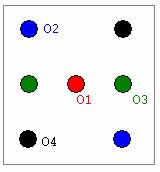
Figure 1. LED configuration and corresponding output variables. (diagrams courtesy of Professor Cheever)
Truth Tables and Karnaugh Maps
A truth table for the die function
can be readily obtained by looking at which of the four outputs need to be
turned on (in reality pulled to 0) for the various counter values. Note that the counter resets when it reaches
6, so the outputs are ‘don’t-cares’. The
die function is completely described in Table 1, and the Karnaugh
maps that are readily obtained from the truth table are shown in Table 2.
|
Counter |
x1 |
x2 |
x3 |
o1 |
o2 |
o3 |
o4 |
|
0 |
0 |
0 |
0 |
1 |
0 |
0 |
0 |
|
1 |
0 |
0 |
1 |
0 |
1 |
0 |
0 |
|
2 |
0 |
1 |
0 |
1 |
1 |
0 |
0 |
|
3 |
0 |
1 |
1 |
0 |
1 |
0 |
1 |
|
4 |
1 |
0 |
0 |
1 |
1 |
0 |
1 |
|
5 |
1 |
0 |
1 |
0 |
1 |
1 |
1 |
|
6 |
1 |
1 |
0 |
x |
x |
x |
x |
Table 1. Truth table for logic function.
|
Output 1 |
x1 \ x2,x3 |
00 |
01 |
11 |
10 |
|
|
0 |
1 |
0 |
0 |
1 |
|
|
1 |
1 |
0 |
x |
x |
|
|
|
|
|
|
|
|
Output 2 |
x1 \ x2,x3 |
00 |
01 |
11 |
10 |
|
|
0 |
0 |
1 |
1 |
1 |
|
|
1 |
1 |
1 |
x |
x |
|
|
|
|
|
|
|
|
Output 3 |
x1 \ x2,x3 |
00 |
01 |
11 |
10 |
|
|
0 |
0 |
0 |
0 |
0 |
|
|
1 |
0 |
1 |
x |
x |
|
|
|
|
|
|
|
|
Output 4 |
x1 \ x2,x3 |
00 |
01 |
11 |
10 |
|
|
0 |
0 |
0 |
1 |
0 |
|
|
1 |
1 |
1 |
x |
x |
Table 2. Karnaugh maps for die logic functions
From the Karnaugh map encirclements (indicated above by bold/italic/underline combinations), the logic functions for O1…O4 are obtained. The boolean SOP expressions are given below.
O1 = ~x3
O2 = x1 + x2 + x3
O3 = x1*x3
O4 = x1 + x2*x3
To drive the LEDs, the outputs had to be inverted. Inverting the expressions obtained above resulted in the set below. These equations
~O1 = x3
~O2 = ~(x1 + x2 +
x3)
~O3 = ~(x1*x3)
~O4 = ~(x1 + x2*x3)
= ~x1*~(x2*x3)
From these equations, the circuit can be readily generated. The only gates used were 3 2-input NAND and 2 3-input NOR gates, for a total of 5 gates in the circuit. This was implemented on the breadboard using 2 TTL ICs. The 3rd input to NOR2 was unused and connected to ground. The schematic of the circuit is shown below in Figure 2.
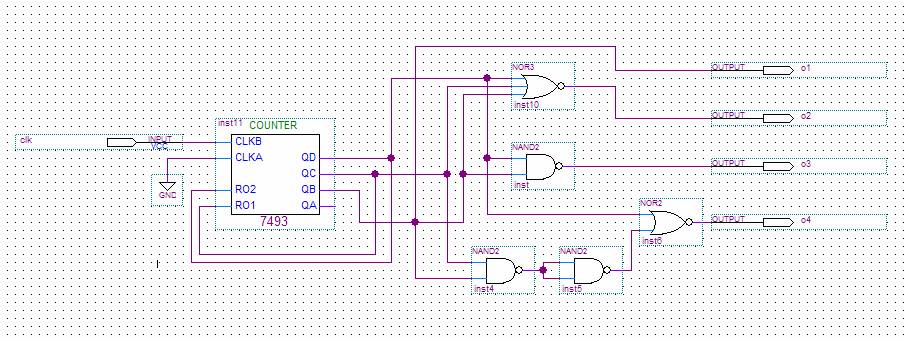
Figure 2. Circuit Schematic (Outputs inverted for correct LED operation)
Quartus II Simulation
To test the circuit, the clk signal was toggled to step the counter.
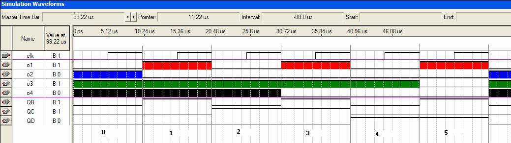
Figure 3. Simulation waveform
of circuit in Figure 2. (Inverted logic outputs for LEDs)
When the outputs are high, the corresponding color is filled in on the waveform below. A quick check when the counter outputs the value 2 indicates that the circuit is operating correctly.
Counter Value = 2
O1 = 0
(LED on)
O2 = 0
(LED on)
O3 = 1
(LED off)
O4 = 1
(LED off)
The LEDs that would be lit up corresponding to this output are shown in Figure 3, and comparing to the definition given in the overview section, the result is indeed correct.
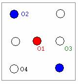
Figure 4. Die lights for Counter = 2.
Further verification of the circuit’s operation was provided in person by Professor Cheever.
Loaded Die
In order to weight the die to cause 1 to show 7 out of 32 rolls and each of the other numbers to show 5 out of 32 rolls, a 5-bit counting system is needed. The Karnaugh map of the numbers represented can be found in Appendix A. Numbers were grouped in an effort to minimize the number of prime implicants needed. Outputs are the same as those used in our implementation of the unweighted die. With the numbers selected as specified in Appendix A, sum-of-products formulas for the outputs are:
O1 = x1 + x2~x3x4~x5
O2 = ~x1 + x2 +
x3x4~x5
O3 = ~x1~x2 +
~x1x3x4 + ~x1x4~x5 + x1x2~x3
O4 = ~x1x3x4 + ~x1~x2x4~x5
Extras
Do a design that uses
minimal logic chips (this may be different than the minimal SOP result).
The complete circuit design consisted of two logic chips (not including the counter): a 7400 quad 2-input NAND and a 7427 triple 3-input NOR. This is the minimal amount of chips to simulate a die.
Can you simplify the circuit
based on the fact that you have multiple outputs?
The circuit could have been simplified by sharing the common ~x1 term in O2 and O4.
In the diagrams above
I used the lights a and g for both count 1 and count 2
(numbers 2 and 3 on the die), but you could use a and g for one of them and b
and f for the other. Can this reduce
logic?
Yes, this reduces the logic. The outputs O2 and O4 simplify from 3 literals down to 2 literals.
|
Output 1 |
x1 \ x2,x3 |
00 |
01 |
11 |
10 |
|
|
00 |
1 |
0 |
0 |
1 |
|
|
01 |
1 |
0 |
x |
x |
|
|
|
|
|
|
|
|
Output 2 |
x1 \ x2,x3 |
00 |
01 |
11 |
10 |
|
|
00 |
0 |
1 |
1 |
0 |
|
|
01 |
1 |
1 |
x |
x |
|
|
|
|
|
|
|
|
Output 3 |
x1 \ x2,x3 |
00 |
01 |
11 |
10 |
|
|
00 |
0 |
0 |
0 |
0 |
|
|
01 |
0 |
1 |
x |
x |
|
|
|
|
|
|
|
|
Output 4 |
x1 \ x2,x3 |
00 |
01 |
11 |
10 |
|
|
00 |
0 |
0 |
1 |
1 |
|
|
01 |
1 |
1 |
x |
x |
|
Number |
LEDs |
Output |
|
1 |
d |
~O1 |
|
2 |
a,g |
~O2 |
|
3 |
b,d,f |
~O1,~O4 |
|
4 |
a,b,f,g |
~O2,~O4 |
|
5 |
a,b,d,f,g |
~O1,~O2,~O4 |
|
6 |
a,b,c,d,e,f |
~O2,~O3,~O4 |
O1=~x3 ~O1=x3
O2=x1+x3 ~O2=~(x1+x3)
O3=x1x3 ~O3=~(x1x3)
O4=x1+x2 ~O4=~(x1+x2)

Figure 5. Minimal cost
circuit schematic.
What is the minimal
circuit (i.e., minimal cost) you can come up with using the techniques
described?
The original cost of the circuit was calculated to be:
1 3-input NOR (3)
1 2-in-put NOR (2)
1 Inverter (1)
2 2-input NAND (4)
Total cost: 5 gates + 10 inputs = 15.
This was the lowest cost for our original circuit, but it was implemented with an extra NAND gate with the inputs tied together to replace the inverter, and another 3 input NOR was used in place of the 2 input NOR with one of the inputs tied to ground. This implementation reduced the number of logic ICs to 2, but did necessarily minimize the cost of the circuit using our rudimentary method for cost calculation.
The minimal cost of the circuit was determined to be
2 2-input NOR (4)
1 2-input NAND (2)
Total cost: 3 gates + 6 inputs = 9.
Appendix A: Loaded
Die Tables
|
|
|
|
|
|
|
|
|
|
|
|
|
|
|
N |
|
|
|
|
|
|
|
|
|
|
|
|
|
x1=0: |
x2x3\x4x5 |
00 |
01 |
11 |
10 |
|
x1=1: |
x2x3\x4x5 |
00 |
01 |
11 |
10 |
|
|
00 |
4 |
4 |
4 |
6 |
|
|
00 |
1 |
1 |
1 |
1 |
|
|
01 |
4 |
4 |
6 |
6 |
|
|
01 |
1 |
1 |
1 |
3 |
|
|
11 |
2 |
2 |
6 |
6 |
|
|
11 |
3 |
3 |
3 |
3 |
|
|
10 |
2 |
2 |
2 |
5 |
|
|
10 |
5 |
5 |
5 |
5 |
|
|
|
|
|
|
|
|
|
|
|
|
|
|
|
O1 |
|
|
|
|
|
|
|
|
|
|
|
|
|
x1=0: |
x2x3\x4x5 |
00 |
01 |
11 |
10 |
|
x1=1: |
x2x3\x4x5 |
00 |
01 |
11 |
10 |
|
|
00 |
0 |
0 |
0 |
0 |
|
|
00 |
1 |
1 |
1 |
1 |
|
|
01 |
0 |
0 |
0 |
0 |
|
|
01 |
1 |
1 |
1 |
1 |
|
|
11 |
0 |
0 |
0 |
0 |
|
|
11 |
1 |
1 |
1 |
1 |
|
|
10 |
0 |
0 |
0 |
1 |
|
|
10 |
1 |
1 |
1 |
1 |
|
|
|
|
|
|
|
O1 = x1 +
x2~x3x4~x5 |
|
|
|
|
||
|
O2 |
|
|
|
|
|
|
|
|
|
|
|
|
|
x1=0: |
x2x3\x4x5 |
00 |
01 |
11 |
10 |
|
x1=1: |
x2x3\x4x5 |
00 |
01 |
11 |
10 |
|
|
00 |
1 |
1 |
1 |
1 |
|
|
00 |
0 |
0 |
0 |
0 |
|
|
01 |
1 |
1 |
1 |
1 |
|
|
01 |
0 |
0 |
0 |
1 |
|
|
11 |
1 |
1 |
1 |
1 |
|
|
11 |
1 |
1 |
1 |
1 |
|
|
10 |
1 |
1 |
1 |
1 |
|
|
10 |
1 |
1 |
1 |
1 |
|
|
|
|
|
|
|
O2 = ~x1
+ x2 + x3x4~x5 |
|
|
|
|
||
|
O3 |
|
|
|
|
|
|
|
|
|
|
|
|
|
x1=0: |
x2x3\x4x5 |
00 |
01 |
11 |
10 |
|
x1=1: |
x2x3\x4x5 |
00 |
01 |
11 |
10 |
|
|
00 |
1 |
1 |
1 |
1 |
|
|
00 |
0 |
0 |
0 |
0 |
|
|
01 |
1 |
1 |
1 |
1 |
|
|
01 |
0 |
0 |
0 |
0 |
|
|
11 |
0 |
0 |
1 |
1 |
|
|
11 |
0 |
0 |
0 |
0 |
|
|
10 |
0 |
0 |
0 |
1 |
|
|
10 |
1 |
1 |
1 |
1 |
|
|
|
|
|
|
|
O3 =
~x1~x2 + ~x1x3x4 + ~x1x4~x5 + x1x2~x3 |
|
|
||||
|
O4 |
|
|
|
|
|
|
|
|
|
|
|
|
|
x1=0: |
x2x3\x4x5 |
00 |
01 |
11 |
10 |
|
x1=1: |
x2x3\x4x5 |
00 |
01 |
11 |
10 |
|
|
00 |
0 |
0 |
0 |
1 |
|
|
00 |
0 |
0 |
0 |
0 |
|
|
01 |
0 |
0 |
1 |
1 |
|
|
01 |
0 |
0 |
0 |
0 |
|
|
11 |
0 |
0 |
1 |
1 |
|
|
11 |
0 |
0 |
0 |
0 |
|
|
10 |
0 |
0 |
0 |
0 |
|
|
10 |
0 |
0 |
0 |
0 |
|
|
|
|
|
|
|
O4 =
~x1x3x4 + ~x1~x2x4~x5 |
|
|
|
|
||