
The purpose of this laboratory was to design a simple CPU modeled on a simplified Von Neumann's IAS computer. The CPU was implemented using the dataflow architecture programmed in VHDL. A digital state machine of the CPU, including the fetch-decode-execute cycle was first developed. This state machine was then coded into VHDL. As a significant extension of these principles, a secondary CPU was also designed in order to provide the capability to execute instructions in parallel. Each CPU was then implemented on an Altera FPGA board. The two boards used the EPP Parallel protocol in order to communicate.
The Basic SSC Architecture - The architecture of the SSC (Simple Swarthmore Computer) is a simplified version of the standard Harvard architecture. The SSC has separate data (RAM) and program (ROM) memories, and a few internal registers for data manipulation and control. The internal register organization closely follows that of Von Neumann IAS computer, and a brief outline follows:
The simple instruction set allows for basic arithmetic operations and control. Each instruction has a few bits of opcode that specify the operation to be executed, as well as an immediate operand value or a memory address reference to an operand. Some instructions take no address or operands. The instructions supported can be grouped into the following four categories.
| Group | Opcodes | Opcode field | Address/Data field |
|---|---|---|---|
| Group A | LOAD X | [0:1] | [2:9] |
| Group B |
LOAD M(X) STOR M(X) JUMP M(X) JUMP +M(X) JUMPCARRY M(X) JUMPOFLOW M(X) ADD M(X) AND M(X) | [0:4] | [5:9] |
| Group C |
STORIO LOADIO | [0:4] | Unused in the original SSC, but specify the I/O channel for parallel operations in the parallel SSC configuration (described later). |
| Group D |
INC DEC LSH RSH INV SWAP LOAD M(MQ) | [0:5] | Unused |
A full listing of the instruction set with the machine instructions along with with the assembly code mnemonics is given below.
| BIN | ASM | Description |
|---|---|---|
| 10 | load | LOAD X Load the value X into ACC. |
| 00000 | lea | LOAD M(X) Load the contents of data memory at location X into the accumulator [ACC]. |
| 00001 | sto | STOR M(X) Move the contents of ACC to data memory location X. |
| 00010 | j | JUMP M(X) Take the next instruction from instruction memory location X. |
| 00011 | jmq | JUMP +M(X) Take the next instruction from instruction memory location X, if the number in MQ is non-negative. |
| 00100 | jc | JUMPCARRY M(X) Take the next instruction from instruction memory location X, if the carry flag is set. |
| 00101 | jo | JUMPOFLOW M(X) Take the next instruction from instruction memory location X, if the overflow/underflow flag is set. |
| 00110 | add | ADD M(X) Add the contents of data memory location X to ACC; put the result in ACC. Set flags as appropriate for the events carry/shift out, and overflow/underflow. |
| 00111 | and | AND M(X) AND the contents of ACC and the contents of data memory location X. |
| 01000 | outb | STORIO Write the value in ACC to an I/O output port. |
| 01001 | inb | LOADIO Load a value from an I/O device (DIP switches) into the ACC. |
| 110010 | inc | INC Increment ACC, set flag for overflow/underflow. |
| 110100 | dec | DEC Decrement ACC, set flag for overflow/underflow. |
| 110110 | lsh | LSH Shift the contents of ACC left by one bit, set flags for carry out. |
| 111000 | rsh | RSH Shift the contents of ACC right by one bit set flags for carry out. |
| 111010 | inv | INV Invert the contents of ACC. |
| 111100 | swap | SWAP Swap the contents of MQ and ACC. |
| 111110 | leamq | LOAD M(MQ) Load the contents of memory at the location specified by the value in MQ into ACC. |
Parallel Extensions to the Core SSC Implementation - The parallel extensions to the SSC required modifications to the original STORIO and LOADIO commands listed above in the original instruction set. The store (outb) command now uses the lower 5 bits of the instruction to specify either to output data to the hexadecimal 7-segment LED displays (all 0's), or to write to one of 8 buffers to send to the second parallel CPU. A pattern of all 1's causes the data to be sent to the second CPU. The load (inb) instruction was modified similarly. All 0's retrives a byte from the dipswitches on the primary CPU's Altera board. All 1's waits for data arrive from the second CPU. An outline is reproduced below:
| Opcode | Lower 5 bits | Asm | Description |
|---|---|---|---|
| 01000 | 00000 | outb | Write to the LEDs directly |
| 01000 | 01xxx | outbpb [0-7] | Write to one of 8 (xxx) data buffers |
| 01000 | 11111 | sdpcpu | Send data to CPU2 over the parallel bus |
| 01001 | 00000 | inb | Read directly from the dipswitches on the primary Altera board |
| 01001 | 11111 | wdpcpu | Wait for data to arrive to the I/O device from CPU2 over the bus |
For simplicity, the secondary processing unit handled mostly everything within a single I/O component. A 64 bit RAM module was the only other element integrated into the secondary unit. The implementation of the I/O module is explained more specifically in a later section.
The second CPU uses an instruction set different from the primary processor. There were several reasons for making a separate 8-bit instruction set. First, in our case the second CPU would perform fewer functions than the primary CPU. A smaller instruction set also made communication between the two units easier to implement since the I/O units were connected by an 8-bit bus. Finally, since both the eight bit data and instructions were received into the same registers, and eight bit instruction set made sense.
Only the instructions that were used for testing the CPU were created. However, since this is a proof-of-concept design it would be trivial to expand the instruction set. The groupings of the instructions implemented, along with their descriptions, are shown below in Tables *** and ***. These instructions were used to obtain two numbers from the dip switches, average them, and send them back to the primary CPU. Two different "priming" functions were required to get numbers from the dipswitches since, due to poorly debounced buttons, it would be impossible to record two different numbers in quick succession.
| Group | Operation | Opcode Field | Address/Data |
|---|---|---|---|
| A | LHS M(X) RHS M(X) | [7..6] | [5..3] |
| B | ADD M(X1) (X2) | [7..6] | [5..3], [2..0] |
| C | STOREDIPS M(X) SENDIO M(X) | [7..4] | [2..0] |
| D | PRIMEONE PRIMETWO | [7..4] | Unused |
| Opcode | Mnemonic | Description |
|---|---|---|
| 00 | LHS M(X) | Shift the contents of register X left by one bit. Set flags for carry out. |
| 01 | RHS M(X) | Shift the contents of register X right by one bit. Set flags for carry out. |
| 1100 | STOREDIPS M(X) | Store switch values to register X |
| 1101 | PRIMEONE | Light up on 7 segment LEDs, implying waiting for a number. Move to next instruction when left button is pressed. |
| 1110 | PRIMETWO | Same as PRIMEONE, but for the other button. |
| 1111 | SENDIO M(X) | Send register X back to the primary CPU. |
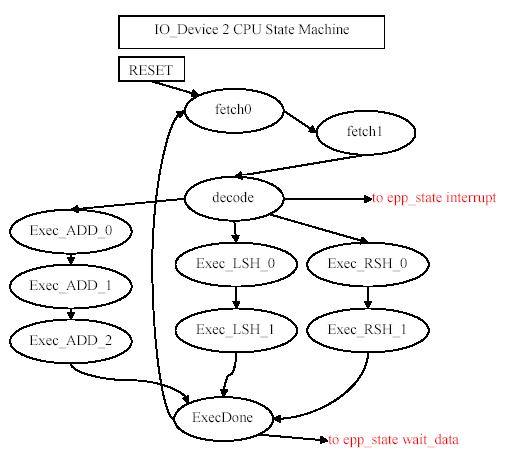
The diagram that follows shows the possible states that the primary (controlling) SSC might be in. The very original SSC implementation had a much larger number of states, but to optimize the execution to take fewer clock cycles per instruction, nearly all redundant states were removed, leaving the following state diagram.
Discussion of Execution Stages - To execute an add instruction, we can simply follow the above state diagram.
To execute an unconditional jump instruction, we again follow the state diagram, ignoring this time the S_Init0 state.
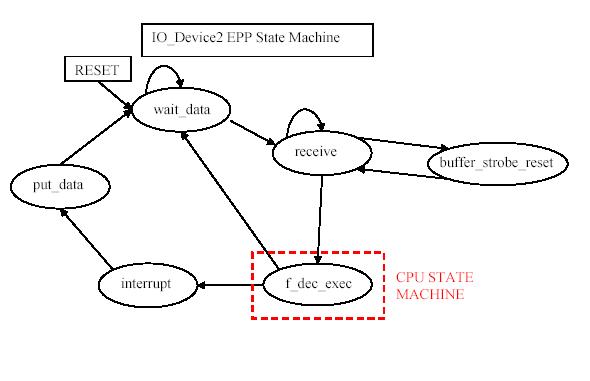
This state machine diagram is the state machine description for the aforedescribed secondary parallel SSC.
The data and program memory modules were implemented using the built-in Altera megafunctions lpm_ram and lpm_rom, respectively. The data memory holds 32 8-bit values, and thus requires 5 bits of addressing. The program memory also holds 32 instructions, but each is 10 bits wide. In order to avoid problems with sychronizing memory accesses, the memories were unclocked and thus functioned asynchronously. It was assumed that after applying an address, the memory value would be available on the data lines on the following clock cycle.
The I/O device connected to the primary CPU had multiple functions. The CPU uses two commands for interfacing with the I/O module. These are the STORIO and LOADIO operations, as described in Table *** on page ***. These functions have to specify the port they are accessing. For the STOREIO command, this allows the CPU to either write to the seven segment displays or to one of the eight buffers used in sending data to the second CPU unit. After the CPU dumps up to 8 bytes of data to the I/O buffers, an access to port "11111" signals the I/O device to send the buffered data to the secondary I/O device.
For loading the data from the I/O device, the CPU either accesses the dip switches or the cached byte sent from the secondary device. The latter operation requires the CPU to wait for a signal from the I/O device indicating it had received the requested data.
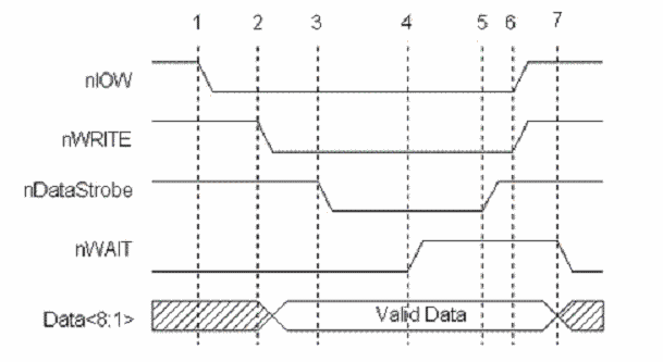
In order for the two I/O devices to communicate, the EPP parallel protocol was used over a bus connecting the two boards. The protocol had to be bidirectional since there were not enough pins connecting the two devices to allow for dedicated single directional lines. The bidirectional requirement severely complicated the programming of the protocol since tri-state buffers with feedback had to be implemented. The buffers were internal to the I/O device and their implementation is described later in the VHDL section. In addition, the protocol was modified by adding a clock signal from the primary CPU to the secondary device in order to assure synchronization. Moreover, this clock had to be slowed down in order to allow full propagation of the assorted signals from one board to another. The diagram and the bus pins used in employing the bi-directional communication protocol are shown in Diagram *** and Table *** below.
| EPP Signal Name | Direction | Description |
|---|---|---|
| nReset | out | Active low. Peripheral reset. |
| nWrite | out | Active low. Indicates a write operation to peripheral. High for a read cycle. |
| nDataStrobe | out | Active low. Indicates a Data_Write operation is in progress. |
| Clk | out | Slowed down clock sent from primary SSC unit. |
| nWait | in | Handshake signal. When low it indicates that is OK to start a cycle (assert a strobe), when high it indicates that it is OK to end the cycle (de-assert a strobe). |
| Intr | in | Peripheral interrupt. Used to generate an interrupt to the host. (Active low in EPP standard, but used as active high in this implementation) |
| Data[7..0] | bi-dir | Bi-directional data lines. |
The secondary I/O device contains the processing unit, so it serves the purpose of both receiving and decoding the instructions. The I/O device is connected to the primary CPU using a parallel data cable and uses the EPP parallel protocol, as described above.
As the data is received into the internal registers of the I/O module, it is immediately written to the 8x8 bit RAM. The lpm_ram function is used to implement the memory storage. Once the data transfer is complete, the I/O component moves into the CPU mode and fetches, decodes, and executes the instructions. Both the instructions and the data are stored in the RAM, so care has to be taken not to clobber needed data or instructions. In this version, there are no jump bits so the program counter is simply incremented after every operation.
When the instruction to send data back to the primary CPU is executed, the I/O device sends an interrupt back to the main device as long as no writing operation is occurring. It then places the data stored in the address specified by the SENDIO function on the bus.
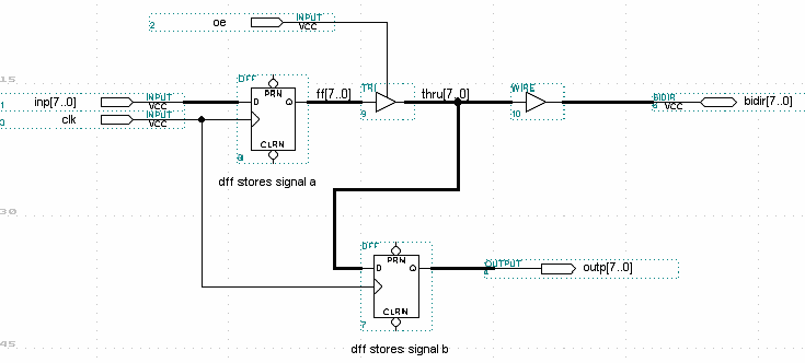
Below is a sample implementation of a tri-state buffer design from the Altera website,.
LIBRARY ieee;
USE ieee.std_logic_1164.ALL;

ENTITY bidir IS
    PORT(
        bidir   : INOUT STD_LOGIC_VECTOR (7 DOWNTO 0);
        oe, clk : IN STD_LOGIC;
        inp     : IN STD_LOGIC_VECTOR (7 DOWNTO 0);
        outp    : OUT STD_LOGIC_VECTOR (7 DOWNTO 0));
END bidir;

ARCHITECTURE maxpld OF bidir IS
SIGNAL  a  : STD_LOGIC_VECTOR (7 DOWNTO 0);  -- DFF that stores
                                             -- value from input.
SIGNAL  b  : STD_LOGIC_VECTOR (7 DOWNTO 0);  -- DFF that stores
BEGIN                                        -- feedback value.
    PROCESS(clk)
    BEGIN
    IF clk = '1' AND clk'EVENT THEN  -- Creates the flipflops
        a <= inp;
        outp <= b;
        END IF;
    END PROCESS;
    PROCESS (oe, bidir)          -- Behavioral representation
        BEGIN                    -- of tri-states.
        IF( oe = '0') THEN
            bidir <= "ZZZZZZZZ";
            b <= bidir;
        ELSE
            bidir <= a;
            b <= bidir;
        END IF;
    END PROCESS;
END maxpld;
Description - The following assembly language program saves a few values into the data memory, loads the value 0, increments it, decrements it, and then proceeds to simply reload the values it saved into data memory before starting over. The Altera simulation results for running this program (after assembling it into machine instructions) follow.
L1:	load 1
	sto 0
	load 2
	sto 1
	load 3
	sto 2
	load 0
	inc
	dec
	lea 0
	lea 1
	lea 2
	j L1
Annotated Simulation Diagram

Discussion of Simulation Results - The above simulation results for the SSC running the simple load/store test program outlined above confirm that the processor correctly executes the instructions. The yellow highlighted register shows the instruction register (IR)'s value as a function of time. The gray highlighted register shows the accumulator's (ACC) values. The brown highlights emphasize any write enables to data memory. The reddish lines denote when a new instruction is loaded into the instruction register, and the blue lines show on which clock cycle the program counter (PC) is updated at the end of each instruction.
The time difference between a blue line forward to the next red line show how many clock cycles are required to fetch and load a new instruction from the program memory. In each case, two clock cycles are needed after the program counter changes before the new instruction is loaded. The time need to execute one instruction can be obtained from the time difference between two red lines. The number of clock cycles required to actually execute each instruction varies with the type of instruction. For example, a STORE (sto) instructions take more clock cycles than an increment instruction since it must set the address and data, and then set the memory write enable signal high. The execution characteristics of each different type of instruction can be thus verified in the simulation.
An instruction-by-instruction description follows.
Assembly Language Description - The SSC assembler provides a quick and easy way to write assembly programs for either the standard original SSC implementations, or with the parallel extensions. The assembler provides some basic error checking, and allows for jumps to mnemonic labels in the source file. A jump command with an argument that begins with an alphabetic character indicates a logical jump to a labeled instruction, while a numeric argument specifies a hard address. Labels must be on a line with an instruction, and must begin with an alphabetic character. Labels cannot have spaces in them and must end directly with a colon ':'. All numeric values must be specified in decimal format (base 10). The values will be converted to the binary 1's and 0's equivalent for the machine instructions. Comments in the assembly begin with a semicolon ';' and extend to the end of the line.
| Mnemonic | Argument | Legal values |
|---|---|---|
| load | IMMEDIATE | 8-bit value (-127 - 126) |
| lea | ADDRESS | 5-bit addr (0 - 31) |
| sto | ADDRESS | 5-bit addr (0 - 31) |
| j | LABEL or ADDRESS | 5-bit addr (0 - 31) |
| jmq | LABEL or ADDRESS | 5-bit addr (0 - 31) |
| jc | LABEL or ADDRESS | 5-bit addr (0 - 31) |
| jo | LABEL or ADDRESS | 5-bit addr (0 - 31) |
| add | OPERAND ADDRESS | 5-bit operand addr (0 - 31) |
| and | OPERAND ADDRESS | 5-bit operand addr (0 - 31) |
| outb | ||
| outbpb | REGISTER ADDRESS | 3-bit data buffer (0-7) |
| sdpcpu | ||
| inb | ||
| wdpcpu | ||
| inc | ||
| dec | ||
| lsh | ||
| rsh | ||
| inv | ||
| swap | ||
| leamq |
The output of the assembler is a 32x8 sized MIF file that can be loaded directly into the program memory of the SSC using the standard Altera lpm_rom LPM_FILE parameter.
To invoke the assembler on a source file:
C:\› sscasm.exe program0.ssc program0.mif
The lab handout was provided by
Professor Maxwell. Professor Maxwell
also oversaw the lab and our progress.
All questions were directed to Professor Maxwell.
The original lab assignment can be found here.