Engineering 72 Lab 2
Aron Dobos, Tyler Strombom -- September 11, 2004
Op-Amps
1a) Inverting Amplifier

Figure 1: Schematic of Inverting Amplifier
- for R2 = 30k Ohms & R1 = 10k Ohms, Vout/Vin = -3
- for R2 = 10 k Ohms & R1 = 10k Ohms, Vout/Vin = -1
1b) Non-inverting amplifier

Figure 2: Schematic of Non-Inverting Amplifier
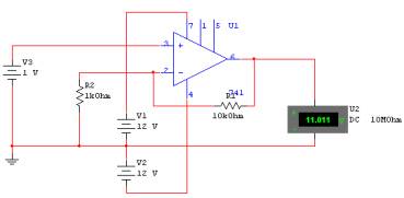
Figure 3: MultiSim Simulation of Non-Inverting Amplifier
1c) Ideal Integrator
- Vout = Vin (-Z2/Z1)
- Z1 = R2
- Z2 = R1 in parallel with 1/sC1
- Vout/Vin = -(R1/R2)/(1+sC1R1)

Figure 4: Schematic of Ideal Integrator
2. Removal of R1
If R1 is removed, Z1 = R2 & Z2 = 1/(sC1). Vout/Vin = -1/sC1R2).
For the ideal integrator, when s = 0 Vout/Vin = -R2 / R1. With R1 removed,
when s= 0 Vout/Vin = infinity. Any small input signal will produce an infinite
output. An infinite output voltage is impossible. Therefore, the output
saturates close to the voltage of the op-amp positive or negative power
supply (L+ or L-).
3. Peak to Peak Amplitude of Triangle Wave Output
The input in the time domain (f(t)) is a unit step.
Taking the Laplace transform, F(s) = 1/s. The transfer
function for the circuit (G(s)) is -1/(sR2C1). The output
function in the frequency domain is found by multiplying
F(s) and G(s), giving -1/(s2R2C1). Taking the inverse
laplace transform, the output function in the time domain
is found to be G(t) = -t/(R2C1). The step occurs over
500 us. R2 = 100k ohms and C1 = .01uF. Plugging in these
values, the peak to peak amplitude of the triangle wave
output is .5 V. This is confirmed by our scope printout
and by our MultiSim simulation.

Figure 5: MultiSim Simulation of Integrator Circuit with Square Wave Input
4. Slew Rate
The manufacturer's slew rate specification for the LM411 is
15 Volts / usec. With a feedback resistor of 30 k, the voltage
transition from +10V to -10V took 960ns, giving a slew rate of
20V/0.96usec = 20.83. Using a 10k feedback resistor, the slew
rate was measured to be 10/1.44 = 6.94 V/usec. The input
resistor in both cases was 10k. This data is interesting because
it seems reasonable that since the slew rate is the ratio of the
voltage drop to the time required for the transition, the slew rate
should be independent of the gain. For the -3 gain circuit, the
slew rate was far higher than for the circuit of -1 gain. This is
probably due to the point at which the time measurements
were made for the smaller gain circuit. Looking at the oscilloscope
printout, the circuit overshot the target voltage of -5 V on the
transition and oscillated slightly before stabilizing at -5V. Our
measurement was taken from the start of the transition to
where the output voltage appeared stable. Had we measured
to the minimum peak voltage value, the time would have been
about 0.7 usec, resulting in a slew rate of 14.28 V/usec, which
is in much greater accordance with the manufacturer's specification.
(So anyways, we probably just measured our time wrong
because it was not clear exactly how the slew rate
measurement was supposed to be made.)
5. Amplifiers with Unity Gain
An amplifier with a gain of 1 might be useful as buffers to separate
parts of circuits. Since the input impedance of an Op Amp is very
high, the Op Amp will not draw large currents from the input circuit
and load it down. That way, the intended operating characteristics
of the input circuit can be maintained and separated from the
output circuit. This could be useful perhaps when designing an
audio amplifier designed to drive large speakers.
6. The Purpose of R3 in the Comparator Circuit
The comparator circuit implemented with an Op Amp operates
by setting a threshold voltage using a voltage divider
between Vcc and Gnd with resistors R1 and R2. Since Vcc
in this case is 5V and R1=R2=10k, the V+ terminal of the
Op Amp is at 2.5V. Since the Op Amp attempts to drive the
two inputs to the same voltage, a voltage less than 2.5V
at the V- terminal will cause the Op Amp output voltage
to saturate at positive supply rail since there is no feedback
resistance. If V- is greater than 2.5, the output voltage
saturates at the opposite supply rail.
Inside the comparator, we can assume that the output is
connected to an internal switch connected to ground.
If V+ > V-, the switch opens, and no current flows from
Vcc through R3 to ground, and the output is essentially
pulled up to Vcc. When the input changes and V+ < V-,
the switch closes and makes short circuit, pulling the
output node to ground. As a result, current flows from
Vcc through R3 to ground, and power is essentially
wasted by R3. As a result, it is desirable to make
R3 large in order to minimize power waste, but a larger
R3 would require the load circuit to have an even
higher impedance to actually realize the full 5V Vcc
on its inputs.
7. The Schmitt Trigger

Figure 6: Schematic of Schmitt Trigger
The Schmitt trigger circuit solves the problem that a
simple comparator exhibits when presented with jittery
input with multiple zero crossings. It does this by
establishing low and high voltage thresholds for the
transition points. Inside the IC, the output is connected
to an internal switch connected to ground. If Vi > V+,
the switch closes, and the output Vo is pulled to ground
(0V). As a result, the terminal voltage at V+ changes,
since instead of just a voltage divider between two 10k
resistors, it is between a R2 (10k) and R1 in parallel
with R3 (5k). The voltage at V+ is now 5/3 V, requiring
that the voltage at Vi drop below 5/3 V to toggle the
output state. Assume now that Vi indeed drops past 5/3
volts. The switch opens, and the output node is no longer
pulled to ground. The voltage at the output node is now
equal to V+ since no current flows through R3. The V+
terminal voltage and Vout return to 5/2V by way of the
10k resistors R2 and R1. That means that the voltage
must increase above 5/2 volts to cause a transition to
the low output state.

For some reason the experimentally measured transition
threshold voltages measured do not correspond with the
theoretical values. Also the output voltage of the
Schmitt trigger does not seem to be 2.5 volts, but
rather something far larger. The low output state
however does seem to go to 0V, as expected. We don't
know how to explain these irregularities. The resistors
were each verified to be 10k.
8. DC Offset on the Signal Generator
The DC offset on the signal generator is required
to push the triangle wave up above 0V so that the
transitions at the edges of the threshold range happen
as the triangle wave changes direction. The DC offset
simply adds a DC voltage to the original triangle wave
signal. Also the DC coupling is required on the
oscilloscope so that it measures absolute voltages and
does not take the average of the maximum and minimum
voltages as the zero point (AC coupling).
9. Relaxation Oscillator

Figure 7: MultiSim Simulation of Circuit
The relaxation oscillator is essentially a Schmitt trigger circuit with the Vin
terminal connected to a resistor R3 and a capacitor C. The RC combination
ensures that the voltage at the Vin terminal cannot change instantaneously,
meaning that it takes time for Vin to transition across the threshold voltage
set at the V+ terminal. The analysis graph above shows clearly the Schmitt
trigger-like transitions of the V+ threshold voltage (green). Refer to the
explanation of the Schmitt trigger circuit for an explanation. When the V+
terminal changes from the low voltage state (~1.2V) to the high voltage state
(~2V), the voltage across the R3 resistor changes, causing more current to flow
through it. Since the voltage across the capacitor cannot change
instantaneously, the capacitor 'fills up' with the time constant defined by RC
in theory until no current flows through it (stable state). However, before it
reaches a stable state, the voltage at the V- terminal of the capacitor will
pass the threshold voltage for the Schmitt trigger, and the V+ voltage and thus
the threshold voltage will drop again. Since the state is now V+ < V-, the voltage at
the output is 0, causing the capacitor to discharge with the same RC time
constant. As soon as the voltage across the capacitor drops below the lower
threshold voltage, the Schmitt trigger flips, and the process repeats.

Figure 8: Scope Printout of Relaxation Operator
(Figure was supplied by David Luong because our
group forgot to include the two input voltages)
The measured time per transition from the above
oscilloscope image shows a period of about ~6 uSec.
The calculated period was 8.06x10^-6, or ~8 uSec.
The theoretical and measured periods are essentially
the same, and the variation in the experimentally
obtained value could easily be a result of resistor
tolerances.