
Figure 1: Oscilloscope Printout of Simple Regulation with Zener Diode
For this rectifier circuit, the input voltage signal is a sinusoid. When the input voltage is positive, current will flow through the diode and the voltage drop across the diode is almost zero and negligible. Therefore, the voltage drop across the resistor (Vout) will be equal to the input voltage. When the input voltage is negative, the diode acts like an open circuit and no current will flow into the resistor. Vout is therefore 0.
For a capacitor placed in parallel with the resistor, Vo(0-) = Vp – Vdiode = Vo (0+). Vo(infinity) = 0 V. The time constant (T) = RC.
Vo(t) = Vo(infinity) + ( V(0)-V(inifinity))*e –t/T
= (Vp-Vdiode)* e –t/T = Vp – Vdiode -Vripple
Vripple = (Vp-Vdiode)*(1- e –t/T)
Period = 1/60 s
where Vripple is the ripple voltage, Vp is the peak voltage for the sinusoid input, and Vdiode is the diode voltage, C is the capacitance, and R is the resistance. Substituting C = 47 uF, R = 470 Ohms, and VP = 10 V for part 2, the ripple voltage is equal to 4.99 volts. Substituting C = 330 uF, R = 470 Ohms, and VP = 10 V for part 3, the ripple voltage is equal to .965 volts.
For part two, the measured ripple voltage is 5 volts compared to the calculated ripple voltage of 4.99 volts. For part three, the measured ripple voltage is .900 volts compared to the calculated ripple voltage of .965 volts.
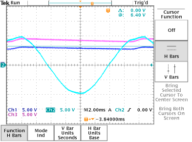
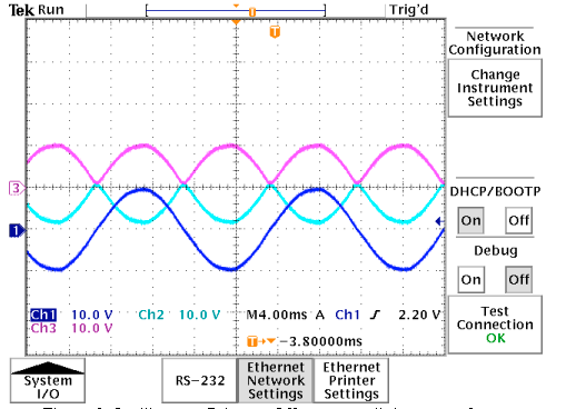
Ch1: Vout, Ch2: Vin, Ch3: Vx
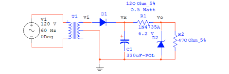
Adding an extra 470 Ohm resistor in parallel to the original load resistor halves the load resistance, and thus doubles the current drain of the load "circuit". As a result, more of the current flowing through R1 is drained in the load, and less through the zener diode. Looking at the current-voltage characteristic of the zener diode, we see that for lower currents, the voltage on the reverse-bias side nears the "knee" voltage, and stops being essentially a constant voltage drop. At the knee, Vo starts to show the voltage ripple at Vx, since the zener diode is no longer functioning in the constant voltage drop zone. This effect can clearly be seen in the following oscilloscope output. The ripple in the output voltage (Ch1) was reached after adding only 1 extra 470 Ohm load resistor in parallel.
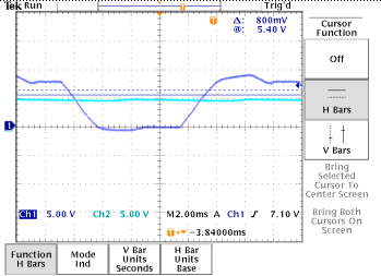
Slight distortions in the output voltage were witnessed with the addition of only one extra 470 Ohm load resistor. However, the ripple was far less than that of the half-wave rectified power supply, since the full-wave rectification generates a much smoother voltage at Vx with the same capacitor because the negative sections of the input sinusoid are inverted, leaving less time for the capacitor to discharge. In the following oscilloscope output, small ripples in the output can be noticed. The horizontal blue cursor line at 5.4 volts indicates the original output voltage under the original load configuration of one 470 ohm resistor.
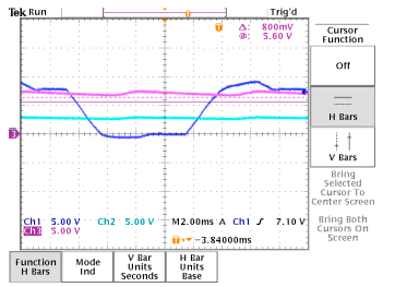
In the following oscilloscope output, 5 additional 470 Ohm load resistors were used. The output voltage retains a slight ripple, but is now only about half of the original output voltage. It is clear that the extra load has caused the zener diode to move inside the knee operating point, resulting in a rather poor power supply.
The circuit will work just as before because the DC voltage will simply pass through the rectifier bridge as if it were a 0 frequency positive-only "AC" signal. However, if the DC polarity is reversed, the attached circuit will still work as before, since the rectifier will invert the polarity change so that current flows through the load in the same direction as it did before. This works by the same reason that the rectifier bridge inverts the negative components of the AC signal to positive. As a result, this circuit can protect small electronics from improperly connected power supplies.
Ch 1: Vin Ch 2: Vout 2 Ch 3: Vout 1
The input is a sinusoid. When the input voltage is positive, the current flows through diode 2 (D2), across R2 and into ground, which creates a positive voltage drop for Vout1. Current is also drawn from ground across R3, which creates a negative voltage drop for Vout2. The current then flows through diode 3 (D3), through the input voltage and into ground. See the following figure for clarification.
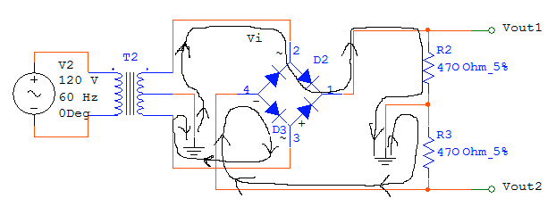
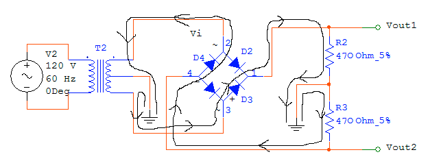
When the input voltage is negative, the current flows through diode 3 (D3), across R2 and into ground, which creates a positive voltage drop for Vout1. Current is also drawn from ground across R3, which creates a negative voltage drop for Vout2. The current then flows through diode 4 (D4), through the input voltage and into ground. See the following figure for clarification.
The full wave rectifier circuit from Part 8 using a center-tapped transformer was joined with the regulated power supply from Part 7. The center-tap was required to provide the positive and negative voltages with the center as the ground. The positive voltage was regulated using the 7805 +5V regulator, and the same capacitor configuration as before. The circuit was "mirrored" for the negative side, but using the 7905 -5V regulator instead. The power supply requirements were to drive a 100 ohm load at 50 mA.
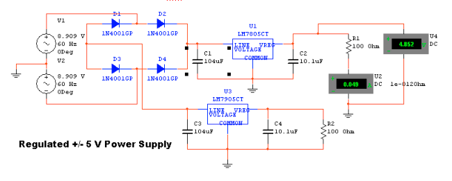
The regulated power supply performs far better than the zener diode regulated supply. When 5 470 Ohm resistors were put in parallel as the load (effectively ~94 ohms), the voltage dropped to about half of the original "no load" voltage. The regulated +/- 5V supply did not exhibit such an undesirable voltage drop.
The electrolytic 10 uF capacitor in parallel with the 0.1 uF ceramic disc capacitor in parallel with the load do not change the voltage characteristics of the power supply circuit. They help provide a consistent current to the load. Electrolytic capacitors respond especially to low frequency (close to DC) current drains and can supply large currents. However, the ceramic disc capacitor is required in case the load circuit drains short pulses of current, since it can respond to much higher frequencies. A microprocessor on a clock drains minimal current between clock cycles, but on the clock’s rising edge, all of the circuitry on the chip "turns on". As a result, the current drain appears as a series of spikes. In order to design the voltage regulation part of the power supply, it is safe to neglect these capacitors, and to focus on the simplified circuit below. The goal is to determine the minimum capacitor value for C1 to maintain a steady voltage output.
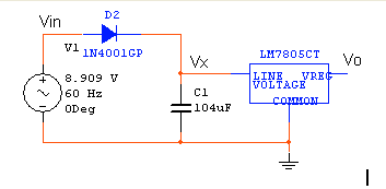
The input voltage from the transformer Vin is 60 Hz 6.3 V RMS. The peak voltage of the sinusoid is thus 6.3*sqrt(2) = 8.909 volts, and is represented by Vm in the following diagram. We can calculate the minimum voltage Vr that Vx may reach and still provide enough voltage to the regulator for a stable 5V output signal by accounting for the 0.7 V diode drop in the rectifier bridge, and the drop off voltage of the 7805. The 7805 datasheet specifies a 1.5 V drop off voltage at 0 mA and 2 V at 1 Amp. At 50mA, the drop off voltage is 1.525 (varies linearly with current). Therefore, Vr must be at least 6.525 V. Calculating the minimum capacitor for these requirements is a straightforward ripple calculation. The governing equation is
which can be approximated by the following assuming that the ripple is small (T< Plugging in appropriate values, we get C = 104 uF. In simulation, the 104 uF
capacitor showed slight glitches (below). Replacing the capacitor with 150 uF
resulted in a completely smooth output voltage (also shown below). The current
drain through the 100 ohm load resistor was 0.049 A, which is indeed what the
design requirements dictated. The input voltage signal is a sinusoid. When the input voltage is positive,
there is a negative feedback loop. When there is a negative feedback loop,
we know that both of the input voltages to the OpAmp are the same voltage,
making the output voltage (Vo) the same magnitude as the input voltage (Vi).
Because there is a .6 volt drop associated with the diode, the output voltage
of the OpAmp must be .6 volts larger than Vi. When the input voltage is negative,
the diode prevents current from flowing. Therefore, there is no negative feedback
loop, the inputs to the OpAmp are no longer the same voltage, and Vo is equal to
zero. The OpAmp then amplifies the negative input signal by its gain of near
infinity. However, because an infinite voltage is impossible, the OpAmp saturates
at its negative power supply of -12 volts. This is all demonstrated in Figures
9 and 10. Ch 1: Vin Ch 2: Vx-Output of OpAmp Ch 3: Vout When the input voltage goes from positive to negative, the current simply shuts
off, the output of the OpAmp drops down to -12V and no glitch occurs. However,
when the input voltage goes from negative to positive, the current is switched
back on but the negative voltage of the OpAmp cannot instantaneously switch to
.6 volts (0V + the voltage drop across the diode). In order for there to be an
output voltage for the circuit, the output of the OpAmp must be positive.
Therefore, there is a delay before the OpAmp output can follow the input voltage,
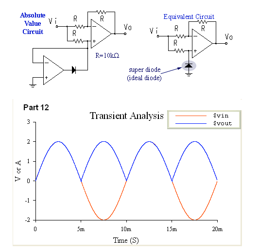
which results in a "glitch" for the output voltage of the entire circuit. The absolute value circuit simply takes the absolute value of the input voltage
and outputs it with no voltage drops. Assuming the super diode circuit works, we
can replace it with a plain diode in the circuit at the right. In this circuit,
if the input voltage is negative, then the diode will conduct, pulling the V+
terminal of the opamp to ground (0V). By the ideal op-amp rule, the negative
input terminal will also be at 0 volts, and we are left with a simple inverting
configuration with a gain of 1. As a result, the output voltage will be the
negative of the (negative) input voltage, giving the inverted output. If the
input voltage is positive, the diode does not conduct, and no current flows
into the opamp nor to ground. Since no current flows through the input and
feedback resistors, there is no voltage drop from Vi to Vo, and as a result
Vo is equal to Vi. The simulation results obtained for the super-diode and absolute
value circuits match closely the behavior observed in lab. (Note:
The absolute value circuit was never actually built in the lab, but
had it been, it probably would have worked.)
Vr = Vm*T/(R*C)
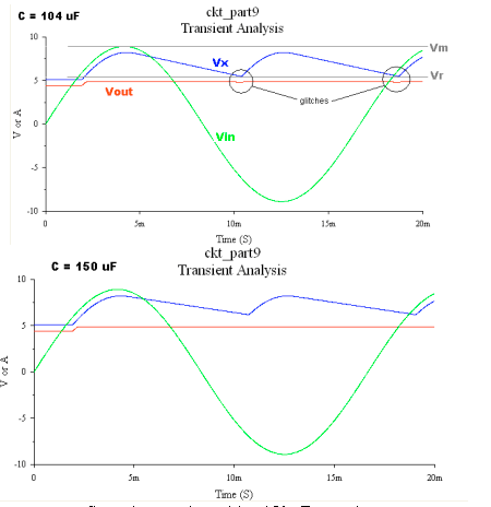
Smooth operation with a 150 uF capacitor
Part 10: How the Precision Rectifier Works

Figure 8: Precision Rectifier for Part 10
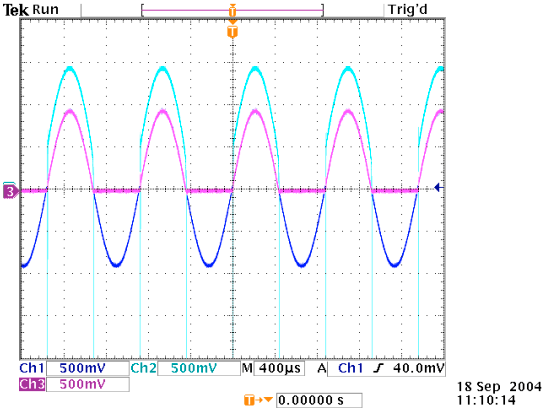
Figure 9: Oscilloscope Printout for Precision Rectifier-Same Scale
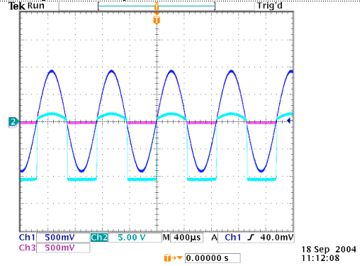
Figure 10: Oscilloscope Printout for Precision Rectifier-different scale
Part 11: Explanation of Glitch
Ch 1: Vin Ch 3: Vout
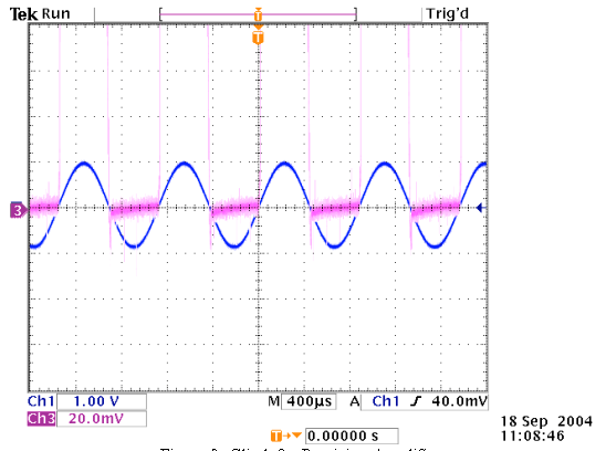
Figure 9: Glitch for Precision Amplifier
Part 12: Driving the Absolute Value Circuit with a 100 Hz Sinusoid
Part 13: Simulation of Super-diode and Absolute Value Circuits
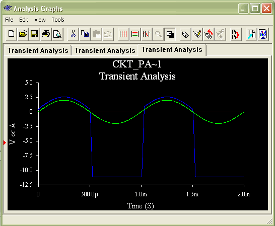
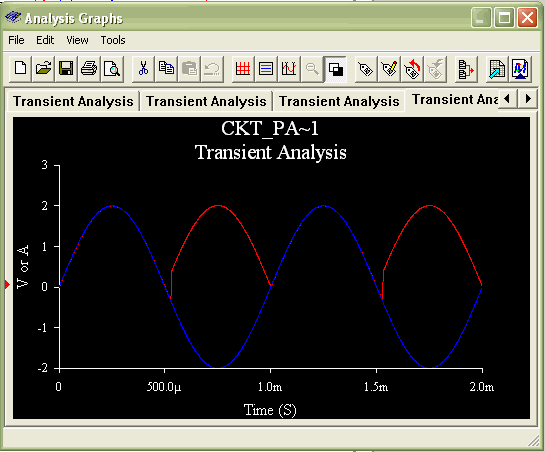
MultiSim Simulation for Part 10: Vi(green), Vx(blue), Vo(red)
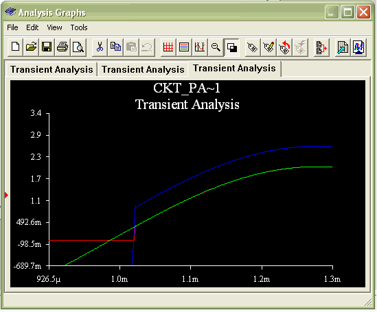
MultiSim Simulation for Part 10-Magnified View of Glitch: Vi(green), Vx(blue), Vo(red)
Multisim Simulation for Part 11- Absolute Value Circuit