Engineering 77 Lab 3
Simple CMOS Layouts
Tyler Strombom, Aron Dobos.
4 October 1955
Abstract
In the lab exercise simple CMOS circuits were designed at the silicon level. Using the L-Edit Layout software, an NMOS transistor, CMOS inverter, 2-input CMOS NAND, and a 2-input CMOS NOR gate were implemented. The correct functioning of the circuits were verified in SPICE using the netlist extracted from the layout tool.
Results
The layout for each circuit is listed below, along with SPICE verification of its operation. The SPICE netlists used are included at the end in Appendix A.
NMOS
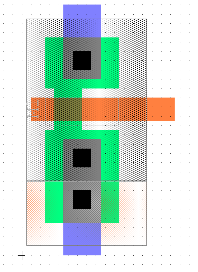
Figure 1. NMOS Layout.

Figure 2. DC Characteristic of NMOS Transistor.
INVERTER
Size: WxH=A 35*40 = 1400 λ2
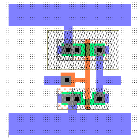
Figure 3. Inverter Layout.
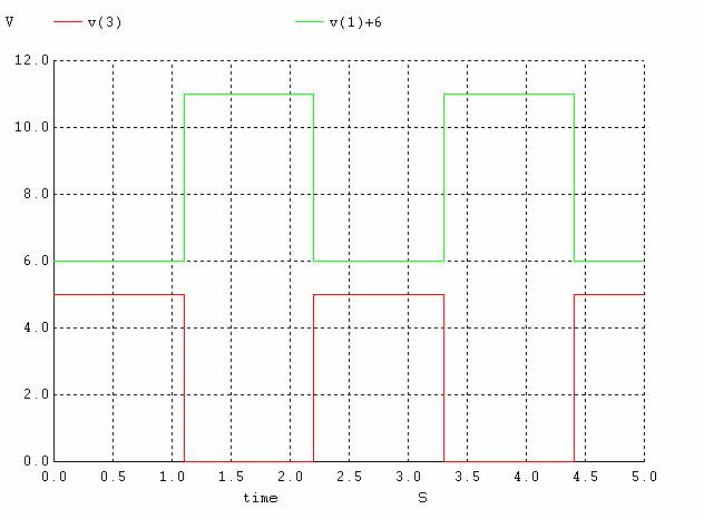
Figure 4. Inverter Transient Analysis.
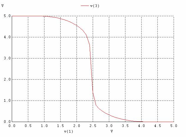
Figure 5. Inverter DC Transfer Characteristic.
NAND2
Size: WxH=A 56*40 = 2240 λ2
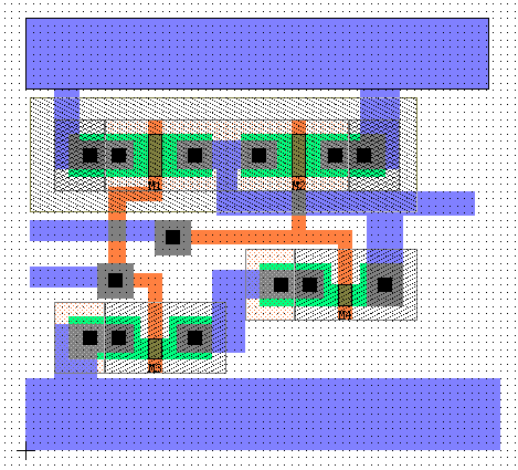
Figure 6. NAND2 Layout.
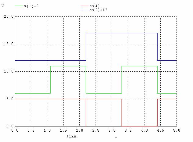
Figure 7. NAND2 Transient Analysis.
NOR2
Size: WxH=A 58*40 = 2320 λ2
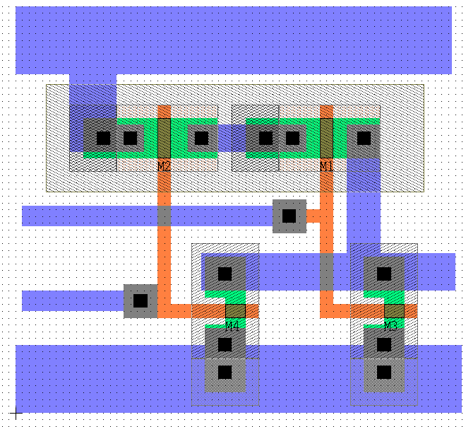
Figure 8. NOR2 Layout.

Figure 9. NOR2 Transient Analysis.
Building a 4 Input CMOS NAND Gate
A 4-input CMOS NAND gate can be constructed using the preexisting 2-input NAND gate using the schematic shown below in Figure 10.
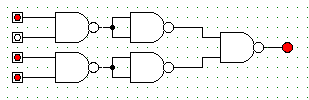
Figure 10. NAND4 Gate Built From NAND2 Gates.
A more efficient implementation could be achieved by replacing the NAND2 gate based inverters with simple CMOS inverters. Since the cells have the same height, the Vdd and GND lines connect directly, and the output of one gate can be connected directly to the input of the next gate from left to right.
If a design is started from scratch, the 2-input design can be extended to a 4-input design by adding two more PMOS and two more NMOS transistors as shown in Figure 11.
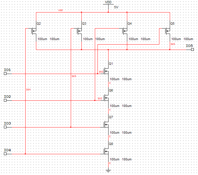
Figure 11. NAND4 Gate At Transistor Level.
A custom design for a 4-input NAND analogous to the 2-input NAND gate can be achieved with the circuit above. The only way for the output (IO5) to be low is if all of IO1..4 are high, since that is the only way a current path is created from Vdd to ground. As a result the circuit functions correctly as a 4 input NAND gate. This approach requires only 8 transistors, while building the gate from smaller components requires a total of 3(4 nand2) +2(2 inverter) =16 transistors. The space savings with a good layout would be significant.
Appendix
A. SPICE Netlists.
NMOS1.CIR
* ledit extract
.MODEL MNMOSIS NMOS LEVEL=2
LD=0.250000U TOX=418.000008E-10
+ NSUB=9.236187E+14 VTO=0.858153
KP=5.048000E-05 GAMMA=0.198
+ PHI=0.6 UO=596.729
UEXP=7.029586E-02 UCRIT=10266.7
+ DELTA=2.7371 VMAX=65701.4
XJ=0.250000U LAMBDA=1.843384E-02
+ NFS=1.086360E+12 NEFF=1
NSS=1.000000E+10 TPG=1.000000
+ RSH=28.760000 CGDO=3.097916E-10
CGSO=3.097916E-10 CGBO=3.838441E-10
+ CJ=8.997900E-05 MJ=0.783638
CJSW=5.524800E-10 MJSW=0.285064 PB=0.800000
.MODEL MPMOSIS PMOS LEVEL=2
LD=0.250000U TOX=418.000008E-10
+ NSUB=9.309300E+15 VTO=-0.889271
KP=1.908000E-05 GAMMA=0.6289
+ PHI=0.6 UO=216.28 UEXP=0.218144
UCRIT=62664
+ DELTA=0.164572 VMAX=100000
XJ=0.250000U LAMBDA=5.011626E-02
+ NFS=9.266623E+11 NEFF=1.001 NSS=1.000000E+10
TPG=-1.000000
+ RSH=66.820000 CGDO=3.097916E-10
CGSO=3.097916E-10 CGBO=3.727276E-10
+ CJ=2.981300E-04 MJ=0.556944
CJSW=3.002100E-10 MJSW=0.243045 PB=0.800000
Vcc 1 0 DC 5
Vin 2 0 DC 1
M1 1 2 0 0
MNMOSIS L=2.5u W=8u AD=44p PD=27u AS=56p PS=30u
* M1 DRAIN GATE SOURCE BULK (12 31
14.5 39)
* Pins of element D2 are shorted:
* D2 1 1
D_lateral AREA=8p
* D2 PLUS MINUS (19 31 20 39)
* Total Nodes: 3
* Total Elements: 2
* Extract Elapsed Time: 0 seconds
.control
dc Vin -2 10 .1
plot -i(Vcc) vs V(2)
.endc
.END
INV1.CIR
* Circuit
Extracted by Tanner Research's L-Edit V7.12 / Extract V4.00 ;
* TDB
File: H:\e77\lab3\inverter, Cell: Cell0
* Extract
Definition File: C:\Documents and
Settings\All Users\Desktop\stu712\mosis\morbn20.ext
* Extract
Date and Time: 10/04/2005 - 21:34
.MODEL
MNMOSIS NMOS LEVEL=2 LD=0.250000U TOX=418.000008E-10
+
NSUB=9.236187E+14 VTO=0.858153 KP=5.048000E-05 GAMMA=0.198
+ PHI=0.6
UO=596.729 UEXP=7.029586E-02 UCRIT=10266.7
+
DELTA=2.7371 VMAX=65701.4 XJ=0.250000U LAMBDA=1.843384E-02
+
NFS=1.086360E+12 NEFF=1 NSS=1.000000E+10 TPG=1.000000
+
RSH=28.760000 CGDO=3.097916E-10 CGSO=3.097916E-10 CGBO=3.838441E-10
+
CJ=8.997900E-05 MJ=0.783638 CJSW=5.524800E-10 MJSW=0.285064 PB=0.800000
.MODEL
MPMOSIS PMOS LEVEL=2 LD=0.250000U TOX=418.000008E-10
+
NSUB=9.309300E+15 VTO=-0.889271 KP=1.908000E-05 GAMMA=0.6289
+ PHI=0.6
UO=216.28 UEXP=0.218144 UCRIT=62664
+
DELTA=0.164572 VMAX=100000 XJ=0.250000U LAMBDA=5.011626E-02
+
NFS=9.266623E+11 NEFF=1.001 NSS=1.000000E+10 TPG=-1.000000
+
RSH=66.820000 CGDO=3.097916E-10 CGSO=3.097916E-10 CGBO=3.727276E-10
+
CJ=2.981300E-04 MJ=0.556944 CJSW=3.002100E-10 MJSW=0.243045 PB=0.800000
M1 3 1 5 5 MPMOSIS L=2u W=6u AD=42p PD=26u AS=36p PS=24u
* M1
DRAIN GATE SOURCE BULK (35.5 36 37.5 42)
M2 3 1 0 0 MNMOSIS L=2u W=3u AD=39p PD=26u AS=33p PS=24u
* M2
DRAIN GATE SOURCE BULK (35.5 13.5 37.5 16.5)
* Pins of
element D3 are shorted:
* D3 2 2 D_lateral AREA=6p
* D3 PLUS
MINUS (28.5 36 29.5 42)
* Pins of
element D4 are shorted:
* D4 1 1 D_lateral AREA=6p
* D4 PLUS
MINUS (29.5 13.5 30.5 19.5)
* Total
Nodes: 4
* Total
Elements: 4
* Extract
Elapsed Time: 0 seconds
Vcc 5
0 DC 5
Va 1 0 PULSE(0 5 1.1 0 0 1.1 2.2)
.control
tran 0.001 5
plot
V(3) V(1)+6
dc Va 0 5 0.1
plot
V(3) vs V(1)
.endc
.END
NAND1.CIR
* Circuit
Extracted by Tanner Research's L-Edit V7.12 / Extract V4.00 ;
* TDB
File: H:\e77\lab3\inverter, Cell: Cell1
* Extract
Definition File: C:\Documents and
Settings\All Users\Desktop\stu712\mosis\morbn20.ext
* Extract
Date and Time: 10/04/2005 - 21:23
.MODEL
MNMOSIS NMOS LEVEL=2 LD=0.250000U TOX=418.000008E-10
+
NSUB=9.236187E+14 VTO=0.858153 KP=5.048000E-05 GAMMA=0.198
+ PHI=0.6
UO=596.729 UEXP=7.029586E-02 UCRIT=10266.7
+
DELTA=2.7371 VMAX=65701.4 XJ=0.250000U LAMBDA=1.843384E-02
+ NFS=1.086360E+12
NEFF=1 NSS=1.000000E+10 TPG=1.000000
+
RSH=28.760000 CGDO=3.097916E-10 CGSO=3.097916E-10 CGBO=3.838441E-10
+
CJ=8.997900E-05 MJ=0.783638 CJSW=5.524800E-10 MJSW=0.285064 PB=0.800000
.MODEL
MPMOSIS PMOS LEVEL=2 LD=0.250000U TOX=418.000008E-10
+ NSUB=9.309300E+15
VTO=-0.889271 KP=1.908000E-05 GAMMA=0.6289
+ PHI=0.6
UO=216.28 UEXP=0.218144 UCRIT=62664
+
DELTA=0.164572 VMAX=100000 XJ=0.250000U LAMBDA=5.011626E-02
+
NFS=9.266623E+11 NEFF=1.001 NSS=1.000000E+10 TPG=-1.000000
+
RSH=66.820000 CGDO=3.097916E-10 CGSO=3.097916E-10 CGBO=3.727276E-10
+
CJ=2.981300E-04 MJ=0.556944 CJSW=3.002100E-10 MJSW=0.243045 PB=0.800000
M1 4 1 5 5 MPMOSIS L=2u W=6u AD=84p PD=52u AS=72p PS=48u
* M1
DRAIN GATE SOURCE BULK (17 38 19 44)
M2 4 2 5 5 MPMOSIS L=2u W=6u AD=72p PD=48u AS=84p PS=52u
* M2
DRAIN GATE SOURCE BULK (37 38 39 44)
M3 3 1 0 0 MNMOSIS L=2u W=3u AD=105p PD=74u AS=105p PS=74u
* M3
DRAIN GATE SOURCE BULK (17 12.5 19 15.5)
M4 4 2 3 3 MNMOSIS L=2u W=3u AD=39p PD=26u AS=105p PS=74u
* M4
DRAIN GATE SOURCE BULK (43.5 20 45.5 23)
* Pins of
element D5 are shorted:
* D5 3 3 D_lateral AREA=6p
* D5 PLUS
MINUS (37.5 20 38.5 26)
* Pins of
element D6 are shorted:
* D6 3 3 D_lateral AREA=6p
* D6 PLUS
MINUS (11 12.5 12 18.5)
* Pins of
element D7 are shorted:
* D7 5 5 D_lateral AREA=6p
* D7 PLUS
MINUS (45 38 46 44)
* Pins of
element D8 are shorted:
* D8 5 5 D_lateral AREA=6p
* D8 PLUS
MINUS (10 38 11 44)
* Total
Nodes: 5
* Total
Elements: 8
* Extract
Elapsed Time: 0 seconds
Vcc 5
0 DC 5
Va 1 0 PULSE(0 5 1.1 0 0 1.1 2.2)
Vb 2 0 PULSE(0 5 2.2 0 0 2.2 4.4)
.control
tran 0.001 5
plot
V(4) V(1)+6 V(2)+12
.endc
.END
NOR1.CIR
* Circuit
Extracted by Tanner Research's L-Edit V7.12 / Extract V4.00 ;
* TDB
File: H:\e77\lab3\lab3, Cell: nor2
* Extract
Definition File: C:\Documents and
Settings\All Users\Desktop\stu712\mosis\morbn20.ext
* Extract
Date and Time: 10/04/2005 - 21:56
.MODEL
MNMOSIS NMOS LEVEL=2 LD=0.250000U TOX=418.000008E-10
+
NSUB=9.236187E+14 VTO=0.858153 KP=5.048000E-05 GAMMA=0.198
+ PHI=0.6
UO=596.729 UEXP=7.029586E-02 UCRIT=10266.7
+
DELTA=2.7371 VMAX=65701.4 XJ=0.250000U LAMBDA=1.843384E-02
+
NFS=1.086360E+12 NEFF=1 NSS=1.000000E+10 TPG=1.000000
+
RSH=28.760000 CGDO=3.097916E-10 CGSO=3.097916E-10 CGBO=3.838441E-10
+
CJ=8.997900E-05 MJ=0.783638 CJSW=5.524800E-10 MJSW=0.285064 PB=0.800000
.MODEL
MPMOSIS PMOS LEVEL=2 LD=0.250000U TOX=418.000008E-10
+
NSUB=9.309300E+15 VTO=-0.889271 KP=1.908000E-05 GAMMA=0.6289
+ PHI=0.6
UO=216.28 UEXP=0.218144 UCRIT=62664
+
DELTA=0.164572 VMAX=100000 XJ=0.250000U LAMBDA=5.011626E-02
+
NFS=9.266623E+11 NEFF=1.001 NSS=1.000000E+10 TPG=-1.000000
+
RSH=66.820000 CGDO=3.097916E-10 CGSO=3.097916E-10 CGBO=3.727276E-10
+
CJ=2.981300E-04 MJ=0.556944 CJSW=3.002100E-10 MJSW=0.243045 PB=0.800000
M1 4 1 5 5 MPMOSIS L=2u W=6u AD=42p PD=26u AS=114p PS=74u
* M1
DRAIN GATE SOURCE BULK (45 37.5 47 43.5)
M2 3 2 4 4 MPMOSIS L=2u W=6u AD=114p PD=74u AS=114p PS=74u
* M2
DRAIN GATE SOURCE BULK (21 37.5 23 43.5)
M3 3 1 0 0 MNMOSIS L=2u W=3u AD=66p PD=48u AS=78p PS=52u
* M3
DRAIN GATE SOURCE BULK (54.5 14 57.5 16)
M4 3 2 0 0 MNMOSIS L=2u W=3u AD=66p PD=48u AS=78p PS=52u
* M4
DRAIN GATE SOURCE BULK (31 14 34 16)
* Pins of
element D5 are shorted:
* D5 4 4 D_lateral AREA=6p
* D5 PLUS
MINUS (51.5 8 57.5 9)
* Pins of
element D6 are shorted:
* D6 4 4 D_lateral AREA=6p
* D6 PLUS
MINUS (28 8 34 9)
* Pins of
element D7 are shorted:
* D7 5 5 D_lateral AREA=6p
* D7 PLUS
MINUS (38 37.5 39 43.5)
* Pins of
element D8 are shorted:
* D8 5 5 D_lateral AREA=6p
* D8 PLUS
MINUS (14 37.5 15 43.5)
* Total
Nodes: 5
* Total
Elements: 8
* Extract
Elapsed Time: 0 seconds
Vcc 5
0 DC 5
Va 1 0 PULSE(0 5 1.1 0 0 1.1 2.2)
Vb 2 0 PULSE(0 5 2.2 0 0 2.2 4.4)
.control
tran 0.001 5
plot
V(3) V(1)+6 V(2)+12
.endc
.END