Engineering 77 Lab 4 Mosfets in the Lab
Aron Dobos, Tyler Strombom
25 October 1955
Abstract
The purpose of this lab was to compare theoretical, experimental, and SPICE generated DC transfer characteristics of an NMOS, PMOS, Inverter, and NAND gate using an ALD1103 chip.
Task 1
To determine VT,n, kn, VT,p, and kp of the NMOS and PMOS transistors in the ALD1103, simples circuit were connected (shown in Figure 1) in which VGS was varied from 0 to 5 volts and VDS was measured. Knowing the precise values of the resistor R and the supply voltage, the transistor current iD was readily calculated.
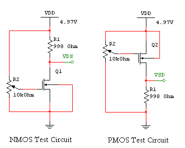
Figure 1. Test Circuits
The measured data values are presented below in Table 1.
|
NMOS |
|
|
PMOS |
|
|
|
Vgs |
Vds |
Id |
Vg |
Vd |
Id |
|
0.09 |
4.97 |
0 |
4.97 |
0 |
0 |
|
0.26 |
4.97 |
0 |
4.78 |
0 |
0 |
|
0.41 |
4.97 |
0 |
4.59 |
0 |
0 |
|
0.5 |
4.97 |
0 |
4.18 |
0.01 |
1E-05 |
|
0.57 |
4.97 |
0 |
4.11 |
0.03 |
3.01E-05 |
|
0.66 |
4.97 |
0 |
4.04 |
0.07 |
7.01E-05 |
|
0.71 |
4.96 |
1E-05 |
3.98 |
0.11 |
0.00011 |
|
0.76 |
4.94 |
3.01E-05 |
3.99 |
0.16 |
0.00016 |
|
0.8 |
4.93 |
4.01E-05 |
3.78 |
0.29 |
0.000291 |
|
0.91 |
4.85 |
0.00012 |
3.65 |
0.45 |
0.000451 |
|
0.98 |
4.76 |
0.00021 |
3.44 |
0.79 |
0.000792 |
|
1.01 |
4.73 |
0.00024 |
3.28 |
1.1 |
0.001102 |
|
1.13 |
4.5 |
0.000471 |
3.04 |
1.6 |
0.001603 |
|
1.3 |
4.07 |
0.000902 |
2.84 |
2.06 |
0.002064 |
|
1.35 |
3.91 |
0.001062 |
2.67 |
2.47 |
0.002475 |
|
1.36 |
3.88 |
0.001092 |
2.35 |
3.21 |
0.003216 |
|
1.41 |
3.72 |
0.001253 |
2.19 |
3.48 |
0.003487 |
|
1.45 |
3.57 |
0.001403 |
1.93 |
3.72 |
0.003727 |
|
1.5 |
3.39 |
0.001583 |
1.67 |
3.86 |
0.003868 |
|
1.62 |
2.92 |
0.002054 |
1.35 |
3.98 |
0.003988 |
|
1.8 |
2.08 |
0.002896 |
|
|
|
|
1.94 |
1.39 |
0.003587 |
|
|
|
|
2.08 |
0.87 |
0.004108 |
|
|
|
|
2.18 |
0.71 |
0.004269 |
|
|
|
|
2.29 |
0.63 |
0.004349 |
|
|
|
|
2.45 |
0.54 |
0.004439 |
|
|
|
|
2.63 |
0.47 |
0.004509 |
|
|
|
|
2.78 |
0.44 |
0.004539 |
|
|
|
|
2.97 |
0.4 |
0.004579 |
|
|
|
|
3.28 |
0.35 |
0.004629 |
|
|
|
|
3.55 |
0.32 |
0.004659 |
|
|
|
|
3.83 |
0.29 |
0.004689 |
|
|
|
|
4.19 |
0.27 |
0.004709 |
|
|
|
Table 1. Measured Voltages for the NMOS and PMOS Test Circuits
Parameters VT,n, kn, VT,p, and kp can be calculated from the data values by guessing which mode the transistor is operating in and plugging in values into the MOSFET equations and solving for the parameter values. The MOSFET equations are reproduced below for reference.

For the NMOS transistor, we assume that the (Vgs, iD) data points (0.91,0.00012) and (0.98, 0.00021) are in the saturation region since we know that VT,n is approximately 0.75V and VDS < VGS-0.75. Therefore we apply the saturation equation and form the system
![]()
Solving, we obtain kn = 0.2642 and VT,n=0.94. For the PMOS transistor, we use the same method, resulting in the equation (Vdd=4.97):
![]()
The results are summarized in Table 2. Since kn and kp were not specified directly in the datasheet, they were calculated from parameters found in the SPICE models. Since the parameters were identical for the NMOS and PMOS models, kn=kp. Given the following equations, the manufacturer k value was derived.
![]()
|
|
VTn |
Kn (A/V2) |
VTp |
Kp (A/V2) |
|
Calculated |
0.9401 |
0.2642 |
-0.9557 |
0.297 |
|
Datasheet |
0.7 |
0.5639 |
-0.7 |
0.5639 |
Table 2. Calculated Transistor Parameters
The calculated values do not agree very well with the specified average values stated by the data sheet, but do indicate that the NMOS and PMOS transistors in the packaged IC are quite well matched. However, the range specified in the datasheet is 0.7 to 1V for VT, so in fact the calculated values are within the allowable range. This makes sense as the datasheet suggests using the ALD1103 for circuits such as a differential pair amplifier in which matched components are essential for proper operation.
The transfer characteristics are given below for the NMOS and PMOS transistors, along with a SPICE simulation using MOSFET models provided by the manufacturer.

Figure 2. NMOS Transfer Characteristic
Figure 3. PMOS Transfer Characteristic
The SPICE decks used for simulation are listed in Appendix A.
Task 2
A derivation of the transfer characteristic of the CMOS inverter using device parameters calculated in Task 1 is given below in Figure 4.
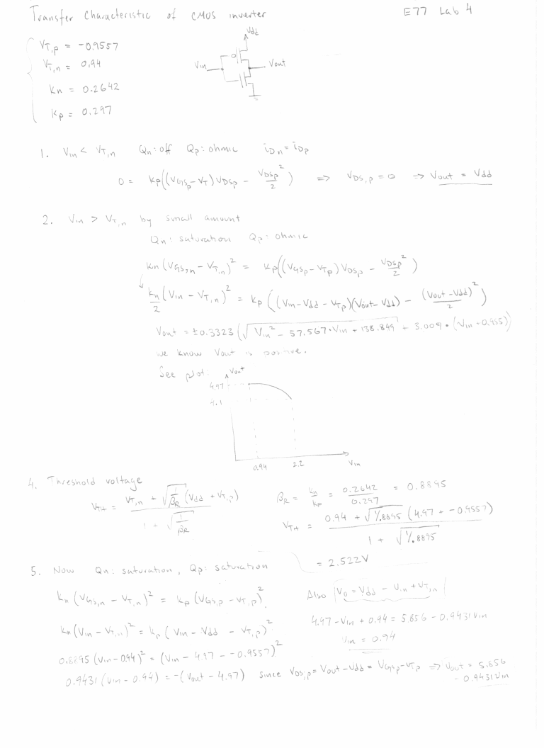
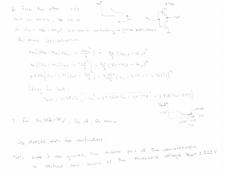
Figure 4. Derivation of CMOS Inverter Characteristic
MATLAB Code For Plotting Analytic Transfer Characteristic
Vin =.94:0.01:2.522;
Vout=.3323*(sqrt(Vin.^2-57.567*Vin+138.849)+3.009*(Vin+.955));
Vin2=2.522:0.01:4.01;
Vout2=-0.3523*(sqrt(-Vin2.^2+57.5548*Vin2-138.798)-2.838*(Vin2-.94));
Vin3=[0 .94];
Vout3=[4.97 4.97];
Vin4=[4.01 4.97];
Vout4=[0 0];
Vin5=[2.52 2.52];
Vout5=[3.594 1.581];
plot(Vin,Vout,Vin2,Vout2,Vin3,Vout3,Vin4,Vout4,Vin5,Vout5)
xlabel('Vin (V)');
ylabel('Vout (V)');
title('Analytic
Solution to Inverter Transfer Characteristic');
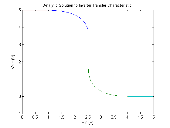
Figure 5. Upper Part of Transfer of Inverter Transfer Characteristic
The experimental result and SPICE simulation are shown below in Figure 6. The hand calculation above yields a threshold voltage VTH = 2.552 that is marginally close to the actual threshold voltage observable in the plot. Of course in the hand calculations the lambda parameter is ignored, accounting for the non-vertical slope of the actual transfer characteristic in the transition region. However, the calculated threshold voltage of the NMOS transistor VT,n=0.94 matches very well the experimental data, as the transistor only starts to conduct right before Vin reaches 1 V, as seen below. The analytic solution suggests that the transistors are much better matched than they seem to be in actuality. This is probably a result of inaccuracies in determining kn and kp in Task 1, since only two data points were used. A more accurate method for determining the parameters from the DC characteristic of the transistors would likely yield better results.
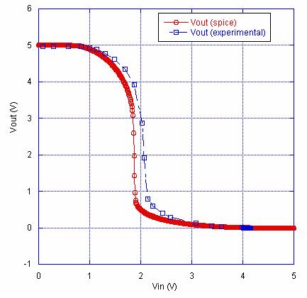
Figure 6. CMOS Inverter, Experimental
Versus Spice Transfer Characteristic
The SPICE netlist used to generate this plot is included in Appendix B.
Task 3
The schematic for the NAND gate is given below.
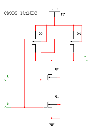
Figure 7. NAND Gate
The truth table for the NAND gate and confirmation of our laboratory built MOSFET NAND gate is provided in Table 3. Note VDD=4.98V. It is clear that the NAND gate is functioning correctly.
|
a |
b |
f |
A (V) |
B (V) |
F (V) |
|
0 |
0 |
1 |
0 |
0 |
4.98 |
|
0 |
1 |
1 |
0.1 |
4.98 |
4.98 |
|
1 |
0 |
1 |
4.98 |
0 |
4.98 |
|
1 |
1 |
0 |
4.98 |
4.66 |
0 |
Table 3. NAND Truth Table
An analytic solution is feasible for the case that both inputs are raised simultaneously from 0 to VDD. In this situation the NAND gate acts as an inverter with the PMOS transistor having twice the width and the NMOS transistor having twice the length of the original inverter circuit. The derivation is identical to that of the inverter but with the length and width parameters appropriately modified. The necessary changes are indicated below.
![]()
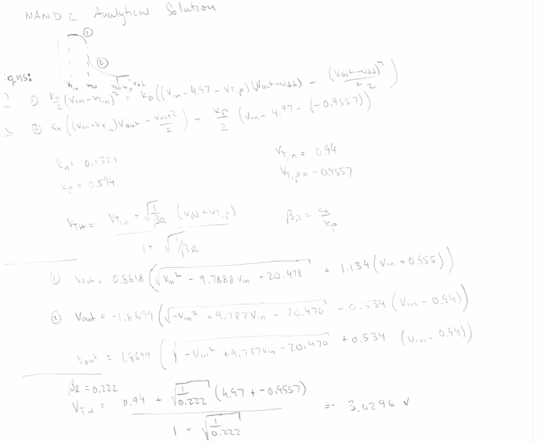
Figure 8. Derivation for NAND2 Analytic Solution
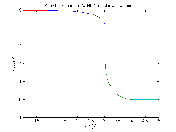
Figure 9. Analytic Solution to NAND2 Gate For Raising
Both Inputs
MATLAB Code For Plotting NAND2 Transfer Characteristic
VTH=3.0296;
Vin =.94:0.001:VTH;
Vout=.8818*(sqrt(Vin.^2-9.7888*Vin+20.478)+1.134*(Vin+.955));
Vin2=VTH:0.001:4.01;
Vout2=-1.8699*(sqrt(-Vin2.^2+9.787*Vin2-20.47)-0.534*(Vin2-.94));
Vin3=[0 .94];
Vout3=[4.97 4.97];
Vin4=[4.01 4.97];
Vout4=[0 0];
Vin5=[VTH VTH];
Vout5=[4.03 1.998];
plot(Vin,Vout,Vin2,Vout2,Vin3,Vout3,Vin4,Vout4,Vin5,Vout5)
xlabel('Vin (V)');
ylabel('Vout (V)');
title('Analytic
Solution to NAND2 Transfer Characteristic');
The switching characteristics are different for the two inputs because the Body effect comes into play with Q2 since the substrate is not connected to the source. As a result the threshold voltage for Q2 changes, affecting the transfer characteristic of the NAND gate depending on which input is toggled. Since the substrate is not tied to ground for Q2, the threshold voltage increases.
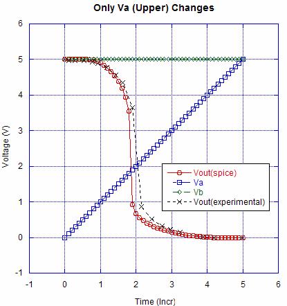
Figure 10. Experimental versus Spice Vout Comparison #1
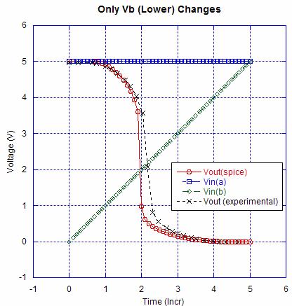
Figure 11. Experimental versus Spice Vout Comparison #2
The threshold voltage is larger when Vb
is the only input that is varied. When Vb
is less than the threshold voltage for NMOS Q1, then Q1 is off and the source
voltage for Q2 is not equal to its base voltage. The body effect occurs,
increasing the threshold voltage for Q2 and thus, increasing the threshold
voltage of the entire NAND circuit.
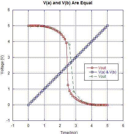
Figure 12. Experimental versus Spice Vout Comparison #3
PMOS Current Mirror
A simple PMOS current mirror was simulated. The ALD1103 chip is designed for such discrete designs because the transistors are matched pairs. Unlike the bipolar transistor current mirror, the MOSFET version of the same circuit has no error in the current transfer from one side of the circuit to the other because of the negligible base current. However, this requires that the MOSFET transistors be well matched so that their DC transfer characteristics are as close to one another as possible (also true for the bipolar circuit). The test circuit is shown below.
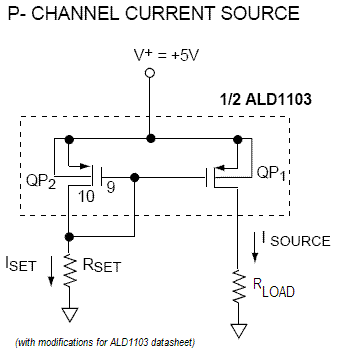
Figure 13. PMOS Current Mirror Test
Circuit

Figure 14. Current matching with 100% matched PMOS transistors
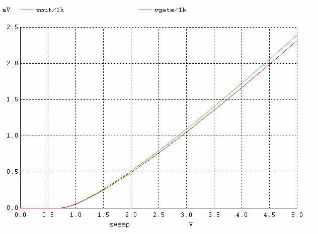
Figure 15. Current matching of PMOS transistor with 0.00005 kp(W/L) error
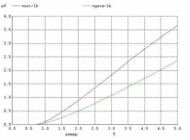
Figure 16. Current matching of PMOS transistor with factor of 2 kp(W/L) error
The current matching worsens linearly with mismatch between the transistors. A 0.00005 error in the kp(W/L) parameter resulted in the mismatch shown in Figure 15, and a factor of 2 error resulted in the characteristic of Figure 16. At Vdd=1.5V, the output current is essentially twice the reference current.
It would have been nice to carry out these experiments in
the laboratory, but due to time constraints it was not possible to test just
how closely the ALD1103 transistors are matched. The discussion above however suggests a
methodology for determining a matching parameter.
Appendix A: Task 1 SPICE Netlists
NMOS.cir
* mosfet device characterization
Vdd
3 0 DC 5
R1
3 2 998
M1
2 1 0 0 NCA-N L=7.8U W=1.11E-3 l=7.8e-6 w=1.106e-3
as=4.825e-8 ps=3.82e-3 ad=1.286e-8 nrd=.3 nrs=1
Vin 1 0 DC 1
*
M1 DRAIN GATE SOURCE BULK
.model
NCA-N nmos (Level=2
+ gamma=1.09 vto=.75
+ Uo=650 Ucrit=0.7e4 Uexp=.1 Vmax=1.6e5
+ phi=.70 tpg=+1 nsub=1e16 neff=10 nss=.7e11 nfs=1.17e11
+ tox=.055u
Cgso=.94n Cgdo=.59n Cgbo=.138n Xqc=.42
+ cj=.39m
mj=.5 cjsw=264p mjsw=0.18
+ xj=2.0u ld=1.6u wd=1.05u
+ pb=.9
js=20.u jssw=2.07e-10 kf=.75e-28 rsh=10)
.model
NCA-P pmos (Level=2
+ gamma=.58 vto=-.74
+ Uo=260 Ucrit=1.0e4 Uexp=.16 Vmax=3.0e5
+ phi=.70 tpg=-1 nsub=1e16 Neff=1 nss=1e11 nfs=1.06e11
+ tox=.055u
Cgso=61n Cgdo=.39n Cgbo=.138n Xqc=.42
+ cj=.18m
cjsw=322p mj=.57 mjsw=0.33
+ xj=1.2u ld=.96u wd=.5u
+ pb=.9 js=20e-6 jssw=2.07e-10 kf=.75e-28 rsh=90)
.control
dc
Vin 0 5 0.01
plot -i(vdd) vs V(1)
plot v(2) vs V(1)
.endc
.end
* mosfet device characterization
Vdd
3 0 DC 4.98
R1
1 0 998
M1
1 2 3 3 NCA-P l=7.8e-6 w=1.106e-3 as=4.825e-8 ps=3.82e-6 ad=1.286e-8 nrd=.3 nrs=1
Vin 2 0 DC 1
*
M1 DRAIN GATE SOURCE BULK
.model
NCA-N nmos (Level=2
+ gamma=1.09 vto=.75
+ Uo=650 Ucrit=0.7e4 Uexp=.1 Vmax=1.6e5
+ phi=.70 tpg=+1 nsub=1e16 neff=10 nss=.7e11 nfs=1.17e11
+ tox=.055u
Cgso=.94n Cgdo=.59n Cgbo=.138n Xqc=.42
+ cj=.39m
mj=.5 cjsw=264p mjsw=0.18
+ xj=2.0u ld=1.6u wd=1.05u
+ pb=.9
js=20.u jssw=2.07e-10 kf=.75e-28 rsh=10)
.model
NCA-P pmos (Level=2
+ gamma=.58 vto=-.74
+ Uo=260 Ucrit=1.0e4 Uexp=.16 Vmax=3.0e5
+ phi=.70 tpg=-1 nsub=1e16 Neff=1 nss=1e11 nfs=1.06e11
+ tox=.055u
Cgso=61n Cgdo=.39n Cgbo=.138n Xqc=.42
+ cj=.18m
cjsw=322p mj=.57 mjsw=0.33
+ xj=1.2u ld=.96u wd=.5u
+ pb=.9 js=20e-6 jssw=2.07e-10 kf=.75e-28 rsh=90)
.control
dc
Vin 0 5 0.01
plot v(2)/998 vs V(1)
plot V(1) vs v(2)
.endc
.end
Appendix B: Task 2 SPICE
Netlists
INV.cir
* inverter transfer characteristic
MPMOS
vout vin
vdd vdd NCA-P l=7.8e-6
w=1.106e-3 as=4.825e-8 ps=3.82e-6 ad=1.286e-8 nrd=.3 nrs=1
MNMOS
vout vin
0 0 NCA-N l=7.8e-6 w=1.106e-3 as=4.825e-8 ps=3.82e-3 ad=1.286e-8 nrd=.3 nrs=1
VVds vdd 0 dc 5
VVin vin 0 dc 3
.model
NCA-N nmos (Level=2
+ gamma=1.09 vto=.75
+ Uo=650 Ucrit=0.7e4 Uexp=.1 Vmax=1.6e5
+ phi=.70 tpg=+1 nsub=1e16 neff=10 nss=.7e11 nfs=1.17e11
+ tox=.055u
Cgso=.94n Cgdo=.59n Cgbo=.138n Xqc=.42
+ cj=.39m
mj=.5 cjsw=264p mjsw=0.18
+ xj=2.0u ld=1.6u wd=1.05u
+ pb=.9
js=20.u jssw=2.07e-10 kf=.75e-28 rsh=10)
.model
NCA-P pmos (Level=2
+ gamma=.58 vto=-.74
+ Uo=260 Ucrit=1.0e4 Uexp=.16 Vmax=3.0e5
+ phi=.70 tpg=-1 nsub=1e16 Neff=1 nss=1e11 nfs=1.06e11
+ tox=.055u
Cgso=61n Cgdo=.39n Cgbo=.138n Xqc=.42
+ cj=.18m
cjsw=322p mj=.57 mjsw=0.33
+ xj=1.2u ld=.96u wd=.5u
+ pb=.9 js=20e-6 jssw=2.07e-10 kf=.75e-28 rsh=90)
.control
destroy all
echo
dc
VVin 0 5 0.01
plot vout vs vin
plot -i(vvds) vs vin
.endc
.end
Appendix C: Task 3
SPICE Netlist
*
Circuit Extracted by Tanner Research's L-Edit V7.12 / Extract V4.00 ;
*
TDB File: H:\e77\lab3\inverter,
Cell: Cell1
*
Extract Definition File: C:\Documents
and Settings\All Users\Desktop\stu712\mosis\morbn20.ext
*
Extract Date and Time: 10/04/2005 -
21:23
.model
NCA-N nmos (Level=2
+ gamma=1.09 vto=.75
+ Uo=650 Ucrit=0.7e4 Uexp=.1 Vmax=1.6e5
+ phi=.70 tpg=+1 nsub=1e16 neff=10 nss=.7e11 nfs=1.17e11
+ tox=.055u
Cgso=.94n Cgdo=.59n Cgbo=.138n Xqc=.42
+ cj=.39m
mj=.5 cjsw=264p mjsw=0.18
+ xj=2.0u ld=1.6u wd=1.05u
+ pb=.9
js=20.u jssw=2.07e-10 kf=.75e-28 rsh=10)
.model
NCA-P pmos (Level=2
+ gamma=.58 vto=-.74
+ Uo=260 Ucrit=1.0e4 Uexp=.16 Vmax=3.0e5
+ phi=.70 tpg=-1 nsub=1e16 Neff=1 nss=1e11 nfs=1.06e11
+ tox=.055u
Cgso=61n Cgdo=.39n Cgbo=.138n Xqc=.42
+ cj=.18m
cjsw=322p mj=.57 mjsw=0.33
+ xj=1.2u ld=.96u wd=.5u
+ pb=.9 js=20e-6 jssw=2.07e-10 kf=.75e-28 rsh=90)
M1
4 1 5 5 NCA-P l=7.8e-6 w=1.106e-3 as=4.825e-8 ps=3.82e-6 ad=1.286e-8 nrd=.3 nrs=1
*
M1 DRAIN GATE SOURCE BULK (17 38 19 44)
M2
4 2 5 5 NCA-P l=7.8e-6 w=1.106e-3 as=4.825e-8 ps=3.82e-6 ad=1.286e-8 nrd=.3 nrs=1
*
M2 DRAIN GATE SOURCE BULK (37 38 39 44)
M3
3 1 0 0 NCA-N l=7.8e-6 w=1.106e-3 as=4.825e-8 ps=3.82e-3 ad=1.286e-8 nrd=.3 nrs=1
*
M3 DRAIN GATE SOURCE BULK (17 12.5 19 15.5)
M4
4 2 3 3 NCA-N l=7.8e-6 w=1.106e-3 as=4.825e-8 ps=3.82e-3 ad=1.286e-8 nrd=.3 nrs=1
*
M4 DRAIN GATE SOURCE BULK (43.5 20 45.5 23)
*
Total Nodes: 5
*
Total Elements: 8
*
Extract Elapsed Time: 0 seconds
Vcc
5 0 DC 4.98
Va
1 0 DC 1
Vb
2 0 DC 1
.control
dc
Va Vb 0 5 0.1
*dc
Vb 0 5 0.1
plot V(4) V(1) V(2)
.endc
.END
Appendix D: Task 4
SPICE Netlist for PMOS Current Source
*
Simple PMOS current source transfer characteristic
VVdds vdd 0 dc 5
* nodes: DRAIN GATE SOURCE BULK
MPMOS1
vgate vgate vdd vdd NCA-P l=7.8e-6 w=1.106e-3
as=4.825e-8 ps=3.82e-6 ad=1.286e-8 nrd=.3 nrs=1
MPMOS2
vout vgate vdd vdd NCA-P l=7.8e-6 w=1.106e-3
as=4.825e-8 ps=3.82e-6 ad=1.286e-8 nrd=.3 nrs=1
Rset vgate 0 1k
Rload vout 0 1k
.model
NCA-P pmos (Level=2
+ gamma=.58 vto=-.74
+ Uo=260 Ucrit=1.0e4 Uexp=.16 Vmax=3.0e5
+ phi=.70 tpg=-1 nsub=1e16 Neff=1 nss=1e11 nfs=1.06e11
+ tox=.055u
Cgso=61n Cgdo=.39n Cgbo=.138n Xqc=.42
+ cj=.18m
cjsw=322p mj=.57 mjsw=0.33
+ xj=1.2u ld=.96u wd=.5u
+ pb=.9 js=20e-6 jssw=2.07e-10 kf=.75e-28 rsh=90)
.control
destroy all
echo
dc
VVdds 0 5 0.1
plot vout/1k vgate/1k
.endc
.end